|
|
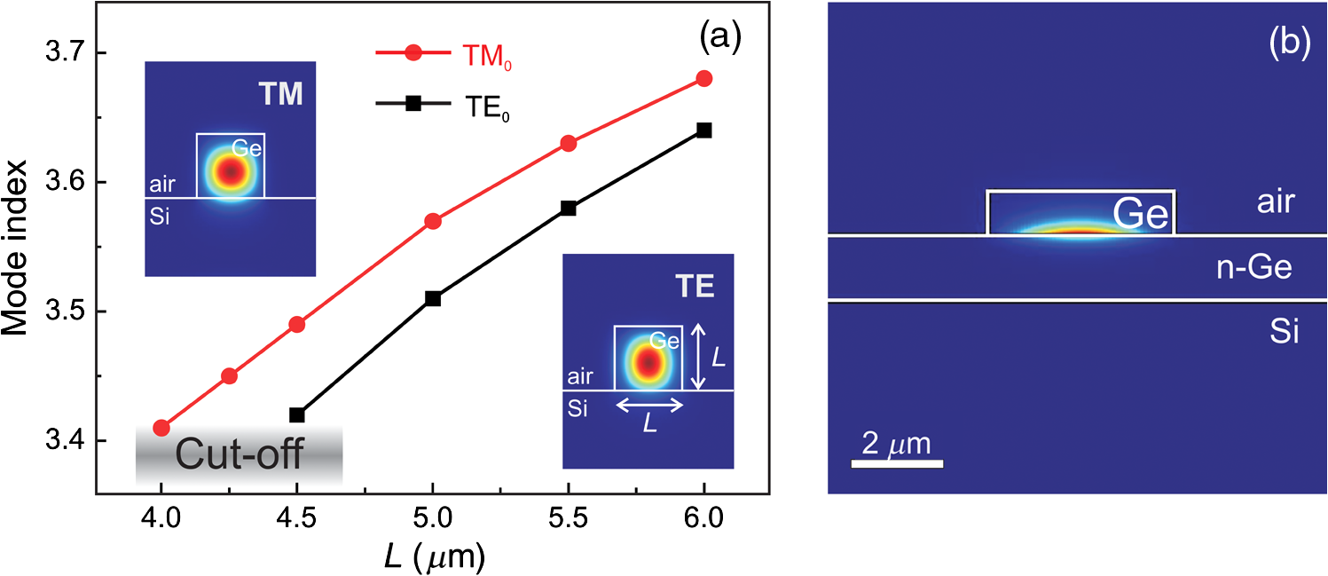
1.IntroductionOver the last two decades, the development of plasmonics for operation around the visible spectral window has heavily relied on gold as the preferred material, mainly because of its excellent properties in terms of stability, easy chemical synthesis, and biocompatibility.1–6 Already in these high-frequency ranges, however, other metals have sometimes been preferred when it comes to specific spectral regions, in particular, Ag and Al for the blue region and, more recently, the near-UV region.7,8 Longer midinfrared (mid-IR) wavelengths have also been approached by exploiting gold,9–13 which in the IR range behaves as a very good conductor, with low penetration depths for the electromagnetic fields. Strictly speaking, however, the equivalent of a plasmonic metal in the mid-IR would possess carrier densities in the to range, something that can be achieved by heavily doping the semiconductor. Indeed, a few seminal works have already outlined the very interesting possibilities that will be opened by the use of such materials for mid-IR plasmonics.14–16 The idea of turning attention to semiconductors as “metals” in the mid-IR comes from the dependence of the plasma frequency (marking the onset of conducting behavior) on the carrier density , according to the relation , where represents the effective mass of the free carriers involved in the plasma oscillations. Another relevant issue when it comes to the use of plasmonic interfaces in optoelectronics and integrated devices is the compatibility with the existing Si photonics and CMOS platforms, something that cannot be solved with Au-based nanostructures. A natural choice in terms of semiconductor materials, from the point of view of integration, points toward Si and Ge.17–19 Between these two, Ge should be preferred both in standard mid-IR photonic devices, due to its inherently lower losses, and for plasmonic applications based on heavy doping, since the lower effective mass ( for Ge compared to for Si) allows a higher plasma frequency to be reached for a given doping level. 2.Material Growth and CharacterizationWe grow epitaxial Ge on standard Si wafers by low-energy plasma-enhanced chemical vapor deposition (LEPECVD).20,21 In an LEPECVD reactor, as sketched in Fig. 1(a), the wafer is exposed to a high intensity plasma, leading to growth rates of several nanometers per second through a very efficient decomposition of the reactive molecules. Since the plasma is obtained by a low-voltage arc discharge, the ion energies are in the range of tens of eV, low enough to allow the growth of crystalline materials. The plasma source is connected to a UHV chamber and the geometry of the plasma is designed by a grounded anode in the lower part of the growth chamber and by a magnetic field induced by a combination of coils and permanent magnets. The reactive gases, , , , and , are fed into the growth chamber through a gas dispersal ring placed above the anode. The dopant gases are diluted in Ar, respectively, 1% and 5%. The substrate is kept at a fixed potential with respect to ground and its temperature is adjusted between 200°C and 750°C by radiation heating. The deposition chamber has a base pressure of , while the working pressure is much higher, reaching . The growth rate is mainly controlled by the plasma density and by the gas flows and it is almost independent from the substrate temperature. For this reason, the growth rate and the surface diffusivity of the adatoms are completely decoupled and they can be optimized separately, a key issue in achieving a high concentration of activated dopants. Moreover, since the decomposition of the reactive molecules is dominated by the plasma, the surface chemistry between the substrate and the reactive molecules plays a modest role in the determination of the alloy composition, which can be easily controlled by the gas flows. The investigated samples were grown on p-type Si(001) substrates with a resistivity of 5 to . Before the heteroepitaxy, the native oxide was removed by dipping the substrate in aqueous hydrofluoric acid solution. All samples were deposited at 500°C at a growth rate of , with a flux of 20 sccm. The highest investigated doping () was achieved in situ by adding 0.15 sccm of . Fig. 1(a) A sketch of the low-energy plasma-enhanced chemical vapor deposition reactor; (b) a sketch of the Fourier-transform infrared spectroscopy setup; (c) the reflectivity spectra for samples with different doping levels; (d) the dielectric constant of the investigated samples extracted from the reflectivity data; (e) a plot of the energy loss function, highlighting the position of the plasma frequency in the investigated materials. 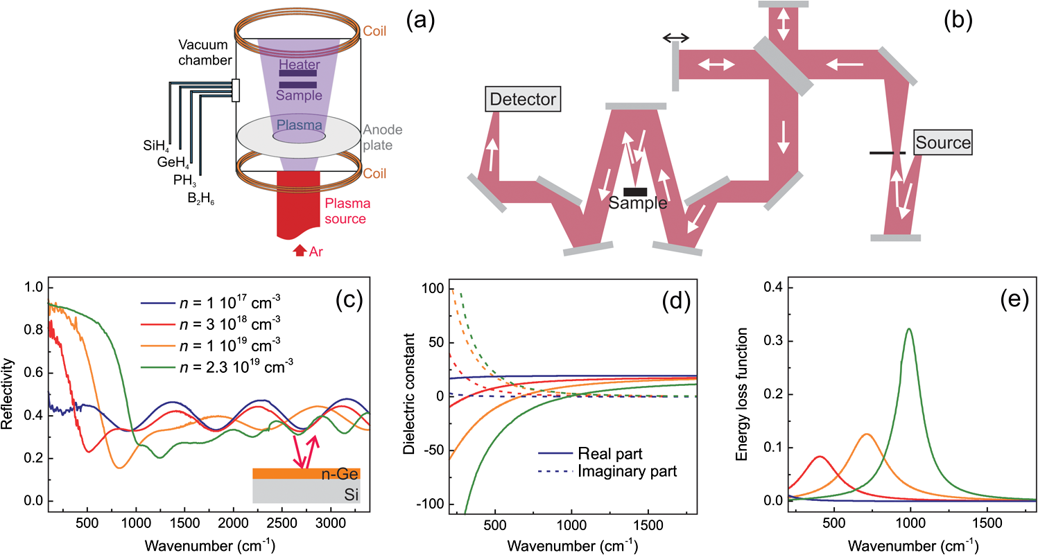 The mid-IR response of materials with different levels of doping in the to range has been characterized by means of Fourier-transform infrared spectroscopy based on a Michelson interferometer, as sketched in Fig. 1(b). Figure 1(c) shows the reflectivity data acquired at near-normal incidence from each sample, after normalization to the reflectivity of a gold mirror. It can already be appreciated that the reflectivity drops from nearly 100% to about 35% when the plasma frequency of the material is crossed and the material’s behavior accordingly turns from metallic (at low frequencies) to dielectric (at high frequencies). In the dielectric region, clear Fabry–Pérot fringes appear because of the finite thickness of the Ge film (1 to for the different investigated samples). By applying a fitting procedure based on multilayer reflectivity and the Drude model, we extract the dielectric function from the experimental data, as demonstrated in Fig. 1(d). In agreement with the above discussion, it can be observed that the real part of the dielectric constant of each sample becomes negative below the corresponding plasma frequency, signifying metallic (plasmonic) behavior. To better highlight the plasmonic response of each material, we plot in Fig. 1(e) the energy loss function, calculated as , which peaks around the plasma frequency because of the energy loss channel opened by bulk plasmons in doped Ge. It can be discovered that the highest doping achieved in this series of samples () places the plasma frequency of Ge around (around wavelength), thus paving the road toward applications of this material platform in mid-IR plasmonics. Doping just above the level is technically achievable and would be sufficient to enable sensing throughout the whole of the important 8 to mid-IR window where many chemical and biological molecules have unique stretching and bending mode molecular absorption lines. 3.Example: Dielectric-Loaded Plasmonic WaveguidesAs a representative example, we consider subdiffraction mode confinement below the dielectric cut-off in coupled metal-dielectric waveguides. In general, the strong reduction of the mode cross section in plasmonic waveguides, which is accompanied by a reduced effective wavelength as well, comes together with significantly increased losses, so that a trade-off between mode volume and propagation length always needs to be considered. For this reason, while standard dielectric waveguides are likely to be the preferred choice for on-chip transmission of signals over footprints that are much larger than the wavelength, plasmonic waveguides could be a choice when strong field confinement, even if only over small distances, is a premium feature, e.g., in integrated sensing applications. From this point of view, the use of a Ge-on-Si platform in the mid-IR allows for the realization of both low-loss dielectric waveguides, with intrinsic Ge already being proposed as one of the key materials for mid-IR waveguiding,19 and plasmonic waveguides, by exploiting heavy n-type doping with P, As, or Sb atoms. Figure 2(a) shows representative data obtained by finite-difference frequency-domain methods22 of the quasidegenerate transverse-magnetic (TM) and transverse-electric (TE) fundamental modes supported by a square dielectric Ge waveguide on a Si substrate, as a function of the side of the waveguide. It can be observed, as expected, that the mode index decreases with the decreasing cross section of the waveguide, until it approaches the index of the substrate and cut-off is reached. For the wavelength used in these simulations, guided modes exist only for waveguide cross sections larger than about , with the mode being the last one to reach cut-off. A standard geometry for subdiffraction plasmonic waveguiding is the so-called dielectric-loaded waveguide,23–25 where a thin dielectric slab is placed on top of a plasmonic film. Figure 2(b) shows that, by exploiting this concept, a Ge dielectric waveguide with a cross section as small as on top of an n-doped Ge film can sustain a propagating plasmonic mode. The dielectric constant of the n-doped Ge is taken from experimental data for the doping level and the index of the supported plasmonic mode is about , confirming that the strong confinement is achieved at the expense of extremely large losses, as is common in most plasmonic waveguides. In perspective, more favorable waveguide geometries allowing for lower losses can be designed. 4.ConclusionsHeavily doped semiconductors might open a new era in mid-IR plasmonics due to the high quality of the material and the possibility of tuning the plasmonic response by controlling the carrier concentration with electrical or optical means. In this frame, the development of a group-IV plasmonic material platform would further benefit from the large integrability and low costs allowed by the compatibility with the Si photonics and CMOS platforms. The present materials already allow operation in the 10 to window, thus, e.g., covering part of the so-called fingerprint region which is of special interest for sensing applications. Future efforts along this road need to be focused on increasing the doping level of Ge and on understanding the sources of losses at mid-IR frequencies in order to optimize the plasmonic material and possibly enter the 5 to wavelength window. AcknowledgmentsThe research leading to these results has received funding from the European Union’s Seventh Framework Programme under Grant Agreement No. 613055. ReferencesE. Ozbay,
“Plasmonics: merging photonics and electronics at nanoscale dimensions,”
Science, 311 189
–193
(2006). http://dx.doi.org/10.1126/science.1114849 SCIEAS 0036-8075 Google Scholar
P. Biagioni, J. S. Huang and B. Hecht,
“Nanoantennas for visible and infrared radiation,”
Rep. Prog. Phys., 75 024402
(2012). http://dx.doi.org/10.1088/0034-4885/75/2/024402 RPPHAG 0034-4885 Google Scholar
V. Giannini et al.,
“Plasmonic nanoantennas: fundamentals and their use in controlling the radiative properties of nanoemitters,”
Chem. Rev., 111 3888
–3912
(2011). http://dx.doi.org/10.1021/cr1002672 CHREAY 0009-2665 Google Scholar
S. Lal, S. Link and N. J. Halas,
“Nano-optics from sensing to waveguiding,”
Nat. Photonics, 1 641
–648
(2007). http://dx.doi.org/10.1038/nphoton.2007.223 1749-4885 Google Scholar
L. Novotny and N. van Hulst,
“Antennas for light,”
Nat. Photonics, 5 83
–90
(2011). http://dx.doi.org/10.1038/nphoton.2010.237 1749-4885 Google Scholar
R. Zia et al.,
“Plasmonics: the next chip-scale technology,”
Mater. Today, 9 20
–27
(2006). http://dx.doi.org/10.1016/S1369-7021(06)71572-3 MATOBY 0096-4867 Google Scholar
F. Bisio et al.,
“Pushing the high-energy limit of plasmonics,”
ACS Nano, 8 9239
–9247
(2014). http://dx.doi.org/10.1021/nn503035b 1936-0851 Google Scholar
J. M. McMahon, G. C. Schatz and S. K. Gray,
“Plasmonics in the ultraviolet with poor metals Al, Ga, In, Sn, Ti, Pb, and Bi,”
Phys. Chem. Chem. Phys., 15 5415
–5423
(2013). http://dx.doi.org/10.1039/c3cp43856b PPCPFQ 1463-9076 Google Scholar
F. Neubrech et al.,
“Resonant plasmonic vibrational coupling in tailored nanoantenna for infrared detection,”
Phys. Rev. Lett., 101 157403
(2008). http://dx.doi.org/10.1103/PhysRevLett.101.157403 PRLTAO 0031-9007 Google Scholar
R. Adato et al.,
“Engineered absorption enhancement and induced transparency in coupled molecular and plasmonic resonator systems,”
Nano Lett., 13 2584
–2591
(2013). http://dx.doi.org/10.1021/nl400689q NALEFD 1530-6984 Google Scholar
R. Adato et al.,
“Ultra-sensitive vibrational spectroscopy of protein monolayers with plasmonic nanoantenna arrays,”
Proc. Natl. Acad. Sci. U. S. A., 106 19227
–19232
(2009). http://dx.doi.org/10.1073/pnas.0907459106 PNASA6 0027-8424 Google Scholar
O. Limaj et al.,
“Midinfrared surface plasmon sensor based on a substrateless metal mesh,”
Appl. Phys. Lett., 98 091902
(2011). http://dx.doi.org/10.1063/1.3559616 APPLAB 0003-6951 Google Scholar
M. Schnell et al.,
“Nanofocusing of mid-infrared energy with tapered transmission lines,”
Nat. Photonics, 5 283
–287
(2011). http://dx.doi.org/10.1038/nphoton.2011.33 1749-4885 Google Scholar
A. Boltasseva and H. A. Atwater,
“Low-loss plasmonic metamaterials,”
Science, 331 290
–291
(2011). http://dx.doi.org/10.1126/science.1198258 SCIEAS 0036-8075 Google Scholar
S. Law et al.,
“All-semiconductor plasmonic nanoantennas for infrared sensing,”
Nano Lett., 13 4569
–4574
(2013). http://dx.doi.org/10.1021/nl402766t NALEFD 1530-6984 Google Scholar
Y. C. Jun et al.,
“Epsilon-near-zero strong coupling in metamaterial-semiconductor hybrid structures,”
Nano Lett., 13 5391
–5396
(2013). http://dx.doi.org/10.1021/nl402939t NALEFD 1530-6984 Google Scholar
D. J. Paul,
“Silicon photonics: a bright future?,”
Electron. Lett., 45 582
–584
(2009). http://dx.doi.org/10.1049/el.2009.1271 ELLEAK 0013-5194 Google Scholar
R. Soref,
“Silicon photonics: a review of recent literature,”
Silicon, 2 1
–6
(2010). http://dx.doi.org/10.1007/s12633-010-9034-y SILIBU 1876-990X Google Scholar
R. Soref,
“Mid-infrared photonics in silicon and germanium,”
Nat. Photonics, 4 495
–497
(2010). http://dx.doi.org/10.1038/nphoton.2010.171 1749-4885 Google Scholar
G. Isella et al.,
“Low-energy plasma-enhanced chemical vapor deposition for strained Si and Ge heterostructures and devices,”
Solid State Electron., 48 1317
(2004). http://dx.doi.org/10.1016/j.sse.2004.01.013 SSELA5 0038-1101 Google Scholar
C. Rosenblad et al.,
“Silicon epitaxy by low-energy plasma enhanced chemical vapor deposition,”
J. Vac. Sci. Technol. A, 16 2785
–2790
(1998). http://dx.doi.org/10.1116/1.581422 JVTAD6 0734-2101 Google Scholar
(2013). Google Scholar
J. Grandidier et al.,
“Dielectric-loaded surface plasmon polariton waveguides: figures of merit and mode characterization by image and Fourier plane leakage microscopy,”
Phys. Rev. B, 78 245419
(2008). http://dx.doi.org/10.1103/PhysRevB.78.245419 PRBMDO 0163-1829 Google Scholar
A. V. Krasavin and A. V. Zayats,
“Three-dimensional numerical modeling of photonic integration within dielectric-loaded SPP waveguides,”
Phys. Rev. B, 78 045425
(2008). http://dx.doi.org/10.1103/PhysRevB.78.045425 PRBMDO 0163-1829 Google Scholar
T. Holmgaard and S. I. Bozhevolnyi,
“Theoretical analysis of dielectric-loaded surface plasmon-polariton waveguides,”
Phys. Rev. B, 75 245405
(2007). http://dx.doi.org/10.1103/PhysRevB.75.245405 PRBMDO 0163-1829 Google Scholar
BiographyPaolo Biagioni is an associate professor in the Physics Department of Politecnico di Milano, Italy. He received his PhD degree in physics from the same institution in 2007 and was then a postdoctoral researcher at the University of Würzburg with a Von Humboldt fellowship. At present, his research interests include nano-optics and plasmonics, with special emphasis on mid-infrared group-IV plasmonics, linear and nonlinear properties of metal nanoantennas, and group-IV nanostructures working at the telecommunication wavelengths. Jacopo Frigerio received his MA degree in physical engineering from Politecnico di Milano and his PhD degree cum laude in physics from Politecnico di Milano. During his PhD, he spent 2 months at the Instituté of Electronique Fondamentale (University Paris Sud) working on electro refraction in Ge quantum wells. His research interests include silicon photonics, thermoelectrics for energy harvesting, plasmonics for mid-infrared sensing applications, and integration of III-V on silicon. Antonio Samarelli received his PhD degree in photonics at the University of Glasgow in 2010. From 2010 to 2014, he was a research associate with the School of Engineering in thermoelectric devices and silicon photonics. He is currently a research fellow for the School of Physics and Astronomy at the University of Glasgow. His current research interests include photonics in the near and mid infrared, plasmonics, MEMS, nanowire and nanofabrication of advanced systems. Kevin Gallacher received his PhD degree from the University of Glasgow, Glasgow, UK, in 2014, on the fabrication and characterization of novel germanium on silicon photonic devices. At present, he is a research assistant at the School of Engineering at the University of Glasgow. Leonetta Baldassarre is a researcher at the Center for Life and Nano Science of the Italian Institute of Technology (IIT) in Rome. She received her PhD degree in materials science in 2008. She was then employed at Universitaet Augsburg and at Elettra Sincrotrone Trieste. She received a national grant for the study of nanometer scale inhomogeneities in strongly correlated electron materials by tip-enhanced infrared spectroscopy. Emilie Sakat received her PhD degree in physics from the Doctoral Graduate School of Polytechnique, France, currently she is a postdoctoral researcher at Politecnico di Milano in Italy. She specializes in plasmonics and nanophotonics for infrared devices. She received the best thesis award from the Airbus Group Foundation for her work on metal dielectric guided mode resonance structures and applications to filtering and infrared imaging. Eugenio Calandrini graduated cum laude in physics at the Sapienza University of Rome in 2014 with a thesis on germanium mid-infrared plasmonics for sensing. Currently, he is enrolled as a PhD student in the Plasmon Technologies Department at the Italian Institute of Technology (IIT) in Genoa. He specializes in plasmonics and nanofabrication. Ross W. Millar received his MEng degree in electronics and electrical engineering from the University of Glasgow in 2012. Currently, he is undertaking his PhD degree in the process-induced straining of germanium near-infrared devices. Valeria Giliberti studied and graduated in physics at the University of Rome La Sapienza in 2011. From the same university, she received her PhD degree in materials science in 2014 for a thesis on nonlinear plasmonic effects in two-dimensional (2-D) electron gases. Currently, she is a postdoctoral researcher in the Physics Department of the University of Rome La Sapienza, where she works in the infrared spectroscopy group. Giovanni Isella received his PhD degree in physics from the Politecnico di Milano, Italy, in 2001. Since 2001 he has been engaged in research on the integration of SiGe heterostructures on Si and their application to micro- and optoelectronics. He was appointed as assistant professor in 2003 and as associate professor in 2014 in the Physics Department at Politecnico di Milano. Douglas J. Paul received his MA and PhD degrees in physics from the University of Cambridge. After spending 20 years in Cambridge, he moved to Glasgow University in 2007 to take up a professorial chair and is now director of the James Watt Nanofabrication Centre. He is fellow of the Royal Society of Edinburgh and the Institute of Physics, he won the President’s Medal in 2014. His research interests include nanoelectronics, SiGe technology, Si photonics, thermoelectrics, and quantum technology. Michele Ortolani is an assistant professor in the Department of Physics, Sapienza University of Rome. He received his PhD degree in materials science in 2005. He was then employed at Elettra Sincrotrone Trieste, at Helmoltz Zentrum Berlin and at the Institute for Photonics and Nanotechnologies of the National Research Council of Italy (CNR-IFN). He received a national grant for the spectroscopic study of the terahertz electrodynamics of 2-D electrons in plasmonic microcavities. |